Overview of Finite Element Ensemble Monte Carlo Device Simulator
Hight Electron Mobility Transistors (HEMTs)
and Metal Semiconductor Field Effect Transistors (MESFETs) are
simulated
using a Monte Carlo Heterojunction 2D Final element (MC/H2F) device
simulator.
Typical features of our Monte Carlo engine in the device simulator include:
- implementation of the finite element mesh for accurate
description of the gate and recess shapes
- inclusion of the external resistances in post-processing
- surface pinning
- analytic non-parabolic three-valley conduction band model for
electrons
- scattering mechanisms in the Monte Carlo module consist
electron interactions with:
- ionized impurities (third-body
exclusion)
- neutral impurities
- elastic acoustic phonons
- piezoelectric deformation potential (if
applicable)
- non-polar optic phonon (intravalley and
intervalley)
- polar optic phonon (intravalley)
- alloy scattering (if applicable)
- impact ionization (if applicable)
- strain effects on electron effective masses, material bandgaps,
optical deformation poptentials, and optical phonon energies are also
included in the InGaAs channel
- gate tunnelling model using the thermionic approach can be
included as an additional simulation process at each time step
Results for the MESFETs grown on GaAs substrate using GaAs/AlGaAs material
system:
- velocity overshoot effects may be engineered by a design of recess region
- surface potential pinning is responsible for the reduction in the drain
current
Results for pseudomorphic HEMTs (PHEMTs) grown
on GaAs substrates with InGaAs channels (for more details look in
papers listed in the Publications
web-page):
- high overshoot velocities in the channel are consistent with measured
characteristics
- effect of velocity overshoot on the direct current (DC) and
radio frequency (RF) performance can be simulated in detail
- introduction of the compressive or tensile strain into the channel
allows to employ a strain engineering in PHEMTs
- channel strain engineering may span a wide spectrum of low mobility values
and high field overshoot characteristics
- complete RF analysis using the Ramo-Shockley theorem can be
compared with experimental results
(
Ultrafast Systems).
- complete study of the double doped design of PHEMTs
- device breakdown investigations due to both impact ionization and
gate tunnelling
- comprehensive study of the electron ballistic transport along the
channel in scaled PHEMTs
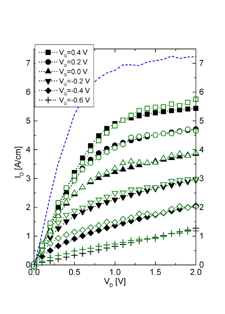
ID-VD characteristics obtained from the
MC/H2F device simulator are calibrated against
experimental data as shown in Fig. 1. after they are remapped by including
external resistances.

|
Figure 1:
I-V characteristic (drain current versus drain voltage) of the
calibrated PHEMT with a gate length of 120~nm. Full symbols represent
experimental data for several fixed gate voltages. Open symbols
represent MC simulations when external resistances of the drain and
source are included. The I-V characteristic for an intrinsic device
(dashed line) is shown for comparison at a gate voltage of 0.4 V.
 Copyright © karolkalna

