Sub 100 nm III-V MOSFETs for Digital Applications
[EPSRC grant No. GR/S61218/01 finished]
III-V MOSFETs for Ultimate CMOS
[EPSRC grant No. EP/F002610/1 finished]
The Device Modelling Part
Motivation
The scaling of the bulk Si MOSFET beyond the 45 nm technology node is extremely difficult due to (i) a low Si mobility and (ii) quantum-mechanical tunnelling through the sub-1 nm thin gate oxide which results in an intolerably high leakage. Therefore, it is widely accepted that the bulk MOSFET architecture has to be dramatically changed and the industry is adopting non-orthodox materials, new technologies and alternative device architectures. Naturally, the research into alternative transistor architectures recreated the possibility of building MOSFET based on III-V materials [1] to profit from a higher mobility in the channel. The development of suitable high-κ gate dielectrics for GaAs with an unpinned oxide/semiconductor interface [2] is recognised as the most important step towards a real III-V transistor as depicted in Fig. 1.Background
Past objections to III-V technologies:
- III-V materials do not have a good native oxide;
- III-V devices have to be grown by epitaxial technology;
- III-V substrates are not in large diameters to offer competitive economies of scale;
- III-V transistors cannot be integrated within the current Si based technology.
- high-κ dielectrics for GaAs/AlGaAs with unpinned oxide/semiconductor interface by Freescale Semiconductor;
- epitaxial SiGe in CMOS;
- alternative device architectures.
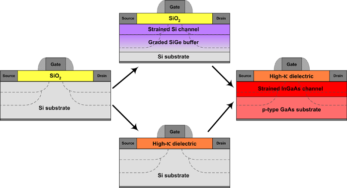 |
Fig. 1: Evolution of technology. The design of the bulk Si MOSFET undergoes changes by replacing SiO2 with high-κ or by replacing Si in the channel with strained Si grown on the graded SiGe buffer. Further improvement in the channel mobility is possible by replacing the strained Si in the channel by the strained InGaAs grown on GaAs buffer. |
Overview
Monte Carlo device simulations show [1,3] that the equivalent III-V MOSFET transistor would outperformed the Si and strain Si MOSFETs when scaled down to a metallurgical gate length of 30 nm but its performance will deteriorate in sub-30 nm dimensions. This decline in performance is associated with a low density of states in III-V materials compared with that of Si and Ge.Modelling approach
We have studied the potential performance of an n-type InGaAs channel MOSFET with an 80 nm physical gate length and a high-κ gate dielectric as depicted in Fig. 2 using ensemble Monte Carlo simulator MC/MOS. We have extended our transport model [4] by using Fermi-Dirac statistics for the screening in ionized impurity scattering and Fermi exclusion principle (degeneracy) at each scattering process [5] . Further, we have incorporated a roughness scattering at the oxide/semiconductor interface and adopted the effective quantum potential to incorporate the effect of quantum confinement. The simulated performance of the InGaAs channel MOSFETs is then compared with the results for equivalent n-type conventional and strained Si channel MOSFETs which have been obtained from calibrated Monte Carlo simulations in order to fairly compare the intrinsic device performance.Features of the Monte Carlo device simulator MC/MOS:
- Finite elements used to depict the complex geometry.
- Analytical non-parabolic band structure with 3 valleys.
- Scattering mechanisms: electron interaction with acoustic phonons, polar optical phonons, non-polar optical phonons (intravalley and intervalley), ionized and neutral impurity scatterings.
- In the InGaAs channel the effect of alloy scattering and the effect of strain on bandgap, electron effective masses, potential and energy of optical phonons are considered.
- Interface roughness.
- Fermi-Dirac statistics.
- Quantum confinement corrections.
Design of equivalent bulk InGaAs MOSFETs
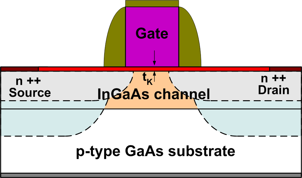 |
Fig. 2: Cross-section of the 80 nm gate length In0.2Ga0.8As MOSFET considered in Monte Carlo simulations. |
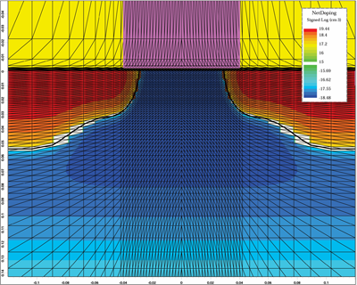 |
| Fig. 3: Doping profile with a peak doping of 5×1019 cm-3 for the 80 nm gate length In0.2Ga0.8As MOSFET considers also the extension regions. |
Performance of the 80 nm gate length In0.2Ga0.8As MOSFETs
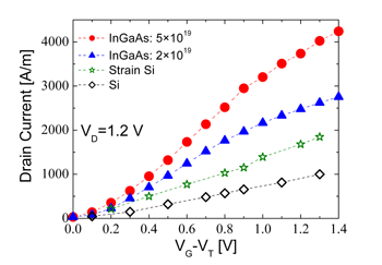
Figures 4 and 5 show ID-(VG-VT) characteristics at drain voltages of 0.1 V and 1.2 V, respectively, for the 80 nm InGaAs MOSFETs. The devices with a source/drain doping of 5×1019 cm-3 would outperform by more than 300% the equivalent strained Si MOSFET at a low drain voltage of 0.1 V. This is reduced to 65% when the source/drain doping is 2×1019 cm-3 which is more realistic for the current technology. At a high drain voltage of 1.2 V the 80 nm InGaAs MOSFETs still outperforms the strained Si MOSFET by more than 200% when the peak doping in the source/drain is 5×1019 cm-3 and by about 50% when this is 2×1019 cm-3.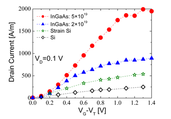 |
 |
|
| Fig. 4: ID-(VG-VT) characteristics of the 80 nm In0.2Ga0.8As MOSFET at a low drain voltage VD=0.1 V compared with the 80 nm Si and strained Si MOSFETs (both have a 67 nm effective channel length). The full circles are for the InGaAs MOSFET with a peak doping of 5×1019 cm-3 while the full triangles are for a peak doping of In0.2Ga0.8As. | Fig. 5: ID-(VG-VT) characteristics of the 80 nm In0.2Ga0.8As MOSFET at a high drain voltage VD=1.2 V compared with the 80 nm Si and strained Si MOSFETs. The full circles are for the InGaAs MOSFET with a peak doping of 5×1019 cm-3 while the full triangles are for a peak doping of In0.2Ga0.8As. | |
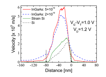 |
| Fig. 6: Average electron velocity along the 80 nm gate length In0.2Ga0.8As channel MOSFETs with the indicated source/drain doping shown by thick full and dash lines compared with the velocity in the equivalent strained Si and Si MOSFETs shown by thin lines. The arrows depict the beginning and the end of the physical gate. |
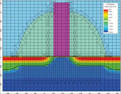 |
| Fig. 7: Doping profile with a peak doping of 5×1019 cm-3 for the 35 nm gate length In0.2Ga0.8As MOSFET obtained from Taurus process simulations. |
Performance of the 35 nm gate length In0.2Ga0.8As MOSFETs
The 35 nm InGaAs MOSFET cannot outperform the equivalent strained Si MOSFETs with more than a 10% Ge content virtual substrate as shown by their ID-(VG-VT) characteristics in Figs. 8 and 9 at both low and high drain voltages, respectively. The 35 nm In0.2Ga0.8As MOSFET with a peak doping of 2×1019 cm-3 is not able to compete even with the bulk 35 nm Si MOSFET. The 35 nm In0.2Ga0.8As MOSFET with a peak doping of 5×1019 cm-3 can outperform the bulk 35 nm Si MOSFET by just 24% while it is outperformed by both strained Si MOSFETs with 10% and 15% Ge content virtual substrates. This performance decline is attributed to a relatively low density of states in In0.2Ga0.8As channel materials when compared to the density of states of Si or Ge. The other factor which is also important is that the n-type doping in the source/drain of the III-V MOSFETs has to be much lower due to technological restrictions than the extremely high doping which can be applied in the equivalent Si and Ge MOSFETs. We would also like to note that the doping designs of both the 80 nm and 35 nm InGaAs MOSFETs have been kept as close as possible to the doping profiles of Si based devices. The performance of the 35 nm InGaAs MOSFETs could be improved if the doping profile would be optimised for the lower density of states in III-V materials.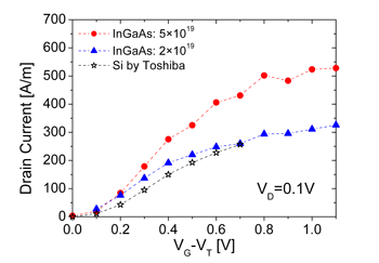 |
 |
|
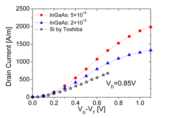
| Fig. 8: ID-(VG-VT) characteristics of the 35 nm In0.2Ga0.8As MOSFET at VD=0.1 V compared with experimental date obtained from the 35 nm gate legnth Si MOSFETs. The two variants of the 35 nm InGaAs MOSFET with peak dopings of 5×1019 cm-3 and 2×1019 cm-3 are shown. | Fig. 9: ID-(VG-VT) characteristics of the 80 nm In0.2Ga0.8As MOSFET at VD=0.85 V compared with the 35 nm gate legnth bulk Si MOSFET. The full circles are for the InGaAs MOSFET with a peak doping of 5×1019 cm-3 while the full triangles are for a peak doping of In0.2Ga0.8As are again presented. | |
Conclusions on scaling of the bulk InGaAs MOSFETs
Using ensemble Monte Carlo device simulations we have demonstrated that compound 80 nm MOSFETs with an In0.2Ga0.8As channel may deliver significant improvement in the drive current compared to the present state of the art bulk and strained Si channel MOSFETs. We have found that the 80 nm InGaAs MOSFET with a source/drain doping of 2×1019 cm-3 would outperform the equivalent Si MOSFET by more than 60% and even by 200% when the source/drain doping is increased to 5×1019 cm-3 at both low and high drain voltages. We have attributed the improvement reported in this work to improved device design and particularly the use of optimal n-type doping in the source/drain and background p-type doping in the design of the InGaAs MOSFET. However, the situation changes for the 35 nm InGaAs MOSFET which cannot outperform the equivalent strained Si MOSFETs with more than a 10% Ge content virtual substrate at any drain voltages even when the extremely high source/drain peak doping of 5×1019 cm-3 is applied. This is attributed to a low density of states in In0.2Ga0.8As channel compared to the density of states in Si and agrees with results reported in Ref. 4.Implant free In0.25Ga0.75As III-V MOSFETs
The introduction of III-V materials in MOSFETs requires new device concepts which enable full exploitation of the high mobility in the scaling process. The new device concept proposed by Frescale Semiconductor [6] is an enhancement mode MOSFET with implant free source/drain regions as shown in Fig. 9. This device contains a buried, high mobility channel formed in a quantum well with energy barriers comparable to the supply voltages at and beyond the 22 nm node. In this way, the carriers are well confined to the channel, providing ultra-thin body like scaling performance. In the access regions, the carriers are supplied to the channel from a doping plane, obviating the need for implanted contact formation and overcoming thermal budget issues associated with efficient implant activation. This results in the carriers being injected at the source side of the gate from a high mobility region, with high velocity and low back-scattering producing very high drive current. The doping strategy is such that the resistance of the access regions either side of the gate is low, whilst under the gate, the structure is normally off, controlled by the work-function of the metal gate. Due to excellent electrostatic integrity and very high channel mobility, the proposed structure tolerates relatively thick gate oxide even at very short gate lengths. This mitigates the impact of the low III-V density of states sustaining very high drive current in nano-scale devices at very low supply voltage.
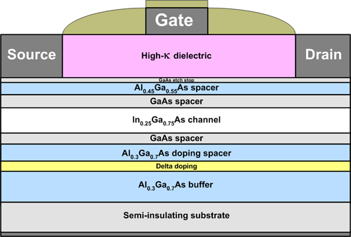 |
Fig. 9 n-type implant free In0.25Ga0.75As MOSFET with a gate length of 100 nm MOSFET considered in Monte Carlo simulations. |
 |
 |
|
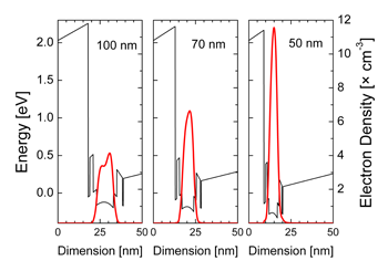
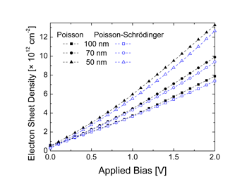
| Fig. 10: Conduction band and electron density in the 100 nm, 70 nm and 50 nm implant free MOSFETs at VG-VT=0.5 V. | Fig. 11: Electron sheet density versus difference between the applied bias and threshold voltage for the 100 nm, 70 nm and 50 nm gate length MOSFETs. The results obtained using both Poisson and Poisson-Schrodinger solutions are shown. | |
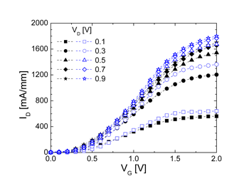 |
Fig. 12: ID-VG characteristics for different drain voltages (VD) of the 100 nm gate length implant free In0.25Ga0.75As MOSFET. The full symbols show the drain current obtained using Boltzmann statistics while the open symbols are results obtained using self-consistent Fermi-Dirac statistics. The source-to-gate and the gate-to-drain distances are set to 100 nm. |
 |
 |
|
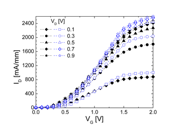
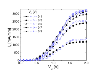
| Fig. 13: ID-VG characteristics for different VD of the 70 nm gate length implant free In0.25Ga0.75As MOSFET. The full symbols show the drain current obtained using Boltzmann statistics and the open symbols using Fermi-Dirac statistics. The source-to-gate and gate-to-drain distances are also scaled to 70 nm. | Fig. 14: ID-VG characteristics for different VD of the 50 nm gate length implant free In0.25Ga0.75As MOSFET. The full symbols represent results of MC simulations using Boltzmann statistics and the open symbols using self-consistent Fermi-Dirac statistics. The source-to-gate and the gate-to-drain distances are 50 nm. | |
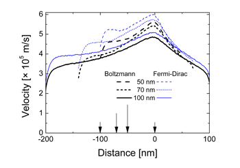 |
Fig. 15: Average electron velocity along the In0.25Ga0.75As channel of scaled implant free MOSFETs with indicated gate lengths at VG-VT=1.3 V and VD=0.7 V. The thick lines are results obtained from MC simulations using Boltzmann statistics while the thin lines are results when Fermi-Dirac statistics is used. The beginning of the gate is depicted by arrows while the end of the gate is always set at zero. |
Conclusions on scaling of the implant free InGaAs MOSFETs
Using ensemble Monte Carlo device simulations we have demonstrated that a 100 nm implant free MOSFET with an In0.25Ga0.75As channel exhibits an excellent drive current of 1650 mA/mm and a maximum transconductance of 1340 mS/mm obtained with a small supply voltage. The MC device simulations have been carefully implemented by:The implant free In0.25Ga0.75As MOSFET has also shown excellent scaling potential. The 70 nm gate length implant free In0.25Ga0.75As MOSFET which is properly scaled in both vertical and lateral directions can deliver a drain current increase of about 50-60% and a maximum transconductance of 2080 mS/mm. When the device is further scaled down to a 50 nm gate length, the drain current increases by about 90-100% compared to the drain current observed in the 100 nm implant free MOSFET and a maximum transconductance of 3190 mS/mm may be achieved.
REFERENCES:
[1][2]
[3]
[4]
[5]
[6]