Click to enlarge
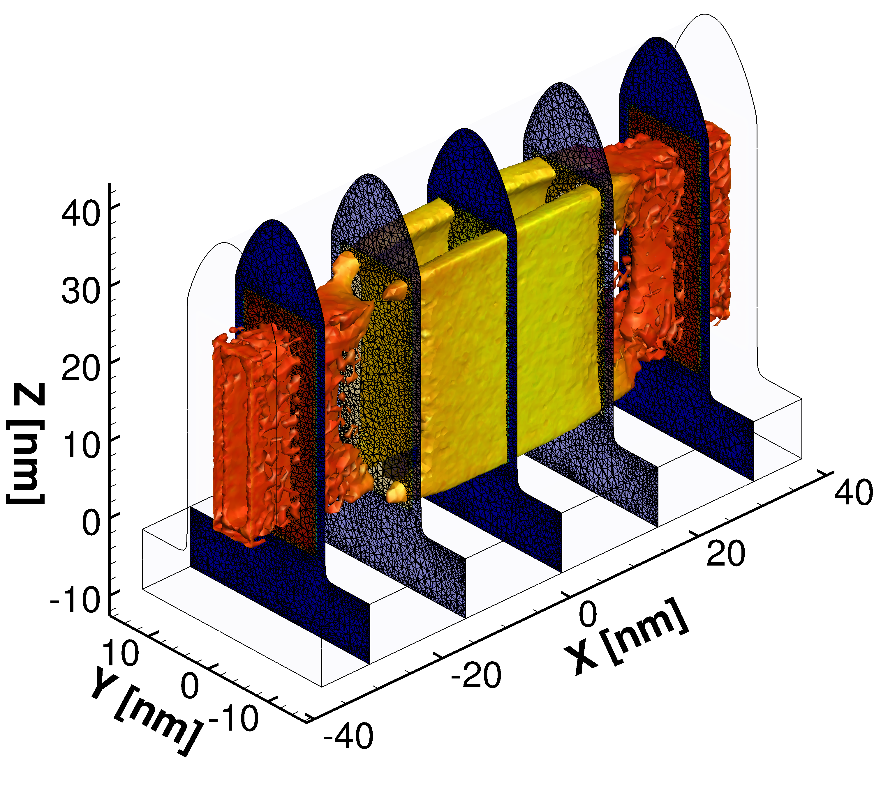
Fig. 1: A 3D simulation domain of the 25 nm gate length Si SOI FinFET showing examples of 2D cross-sections for the solution of Schrödinger equation simulated by VENDES. The electron density illustrating dopants in source/drain is visualised at a high applied drain bias of 1.0 V.
|
The core tools of my device modelling research are:
- a parallel 3D finite element ensemble Monte Carlo device simulation toolbox with integrated 2D finite element Schrödinger equation solutions across channel which can be combined with 3D drift-diffusion simulations (VENDES).
- 2D finite element ensemble Monte Carlo device simulation tool (MC/H2F).
A novel parallel 3D finite element ensemble Monte Carlo device simulation tool MC/P3F was developed to model FinFETs (Fig. 1) and nanowire FETs. The MC/H2F was originally developed to investigate electron transport properties in compound FETs. Later, the code has been rewritten to deal with a MOSFET structure including Si and III-V semiconductors using non-parabolic anisotropic three valleys bandstructure, oxide layer/layers and analytical or imported doping profiles (Fig. 2). The Monte Carlo device simulation tools include self-consistent calculations of the Fermi energy and electron temperature used for ionized impurity scattering and degeneracy (Fermi exclusion principle), interface roughness scattering, interface phonons scattering, on the top of all relevant (intra-valley and inter-valley) electron-phonon scattering mechanisms. The quantum confinement effects are included as quantum corrections using the effective quantum potential in the 2D MOSFET Monte Carlo tool (MC/MOS) and finite element adopted density gradient and 2D Schrödinger equation solutions across channel in the 3D finite element Monte Carlo/Drift Diffusion toolbox (VENDES).
In 2002, the 2D Monte Carlo tool MC/MOS was used to proposed III-V material channel for MOSFETs when scaled into deep sub-100 nm dimensions. This opened research into III-V MOSFETs within the first III-V MOSFET grant "Sub 100 nm III-V MOSFETs for Digital Applications" supported by EPSRC in 2003, followed by the second III-V MOSFET grant"III-V MOSFETs for Ultimate CMOS" funded by EPSRC in 2007 and a FP7 STREP project "DUALLOGIC" funded by EC.
|
|
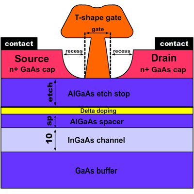
The Monte Carlo simulator MC/H2F forecasted a performance of high electron mobility transistor (HEMTs) scaled into deep sub-100 nm dimensions (Fig. 3). The typical pseudomorphic HEMT simulated using Monte Carlo device simulator has a T-shaped gate; a 30-nm heavily Si-doped 4x1018 cm-3 n+ GaAs cap layer; an Al0.3 Ga0.7As etchstop layer; a 7x1012 cm-2 Si delta doped layer on top of an Al0.3 Ga0.7As spacer layer and, finally, an In0.2Ga0.8As channel. The whole device structure is grown on top of a 50-nm GaAs buffer.
Click to enlarge
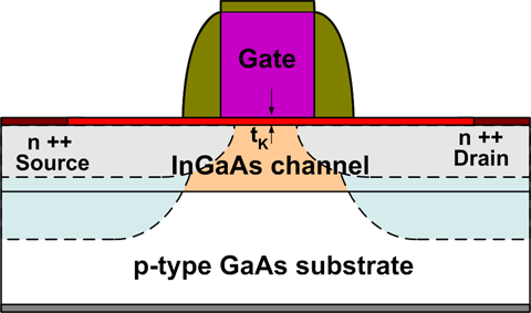
Fig. 2: A cross-section of the proposed III-V MOSFET simulated with the MC/MOS.
The finite element heterostructure ensemble Monte Carlo device simulator uses quadrilateral finite elements to depict a complex geometry of the HEMTs or MOSFETs, and accurately calculates electrostatic effects caused by the gate and recess geometry as well as the surface potential pinning. It is capable of precisely reproducing a T-shape gate and recess formation in the device. The Monte Carlo module includes electron scattering with polar optical phonons; inter- and intra-valley non-polar optical phonons; acoustic phonons; and ionized and neutral impurity scattering. In addition, alloy scattering and strain effects are considered in the InGaAs channel of the device.
|
Click to enlarge
Fig. 3: A cross-section of pseudomorphic high electron mobility transistor simulated with the MC/H2F. |
